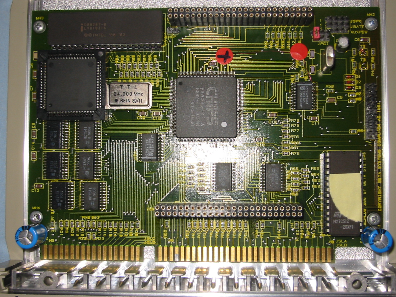
Back to Supercharger!1. The daughter board with the CPU286 in the center and the FPU287 in the top left corner. The quartz is at 24MHz and I suspect the working frequency to be 8MHz as on the mother board because the FPU seems to be a 8MHz one.
Bottom connector looks like a ISA or PCI one: I think this was useful in the development of this board.
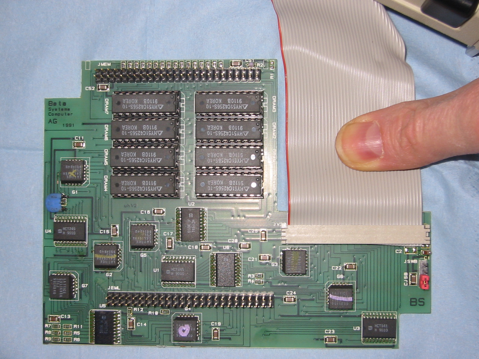
2.The interface card: two rows of connectors are to be plugged into the daughter board, and the grey connector goes to the mother board into the CPU NecV30 socket.
Date is 1991 for this interface.
3.The whole thing: on the left the mother board without its CPU, then the connector to the interface on the right that covers the daughter board with the 286.
Strange thing: the mother board has only 512kb on it, 1Mb would have been better for a 286 system.